++++++++++++++++++++++++++++++++++++++++++++++
Introduction_to_Activities_of_Yoshiaki_Daimon_Hagiwara
Updated on May 4, 2022 at 9:40 a.m. (Japan Time)
Japanese
++++++++++++++++++++++++++++++++++++++++++++++
++++++++++++++++++++++++++++++++++++++++++++++
https://en.wikipedia.org/wiki/Yoshiaki_Hagiwara
Publication_List_by_Yoshiaki_Hagiwara.html
++++++++++++++++++++++++++++++++++++++++++++++
+++++++++++++++++++++++++++++++++++++++++++++++++++++++++
Pinned_Buired_Photodiode_invented_in_1975_and_developed_in_1978_by_Hagiwara_at_Sony.pdf
++++++++++++++++++++++++++++++++++++++++++++++
Who_invented_Pinned_Buried_Photodiode_with_Dyanamic_Charge_Storage_Memory_Capacitor_2022_04_14.pdf
Pinned_Photodiode_with_Dynamic_Charge_Storage_Capacitor_01.pdf
++++++++++++++++++++++++++++++++++++++++++++++
+++++++++++++++++++++++++++++++++++++++++++++++++++++++++
IEEE_ICECET2021_Conference_Paper061_and_Paper075_by_Hagiwara.html
+++++++++++++++++++++++++++++++++++++++++++++++++++++++++
IEEE_EDTM2020_Conference_Paper_by_Hagiwada.html
+++++++++++++++++++++++++++++++++++++++++++++++++++++++++
IEEE_3DIC2019_Conference_Paper_on Multichip CMOS Image Sensor Structure for Flash Image Acquisition (pdf)
+++++++++++++++++++++++++++++++++++++++++++++++++++++++++
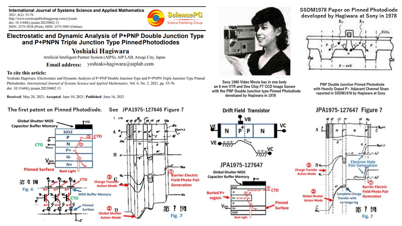
P2021_IJSSA2021_Paper_June_16_2021_on_Electrostatic_and_Dynamic_Analysis_of_Pinned_Photodiodes_22_Pages.pdf
P2021_IJSSA2021_Paper_June_16_2021_on_Electrostatic_and_Dynamic_Analysis_of_Pinned_Photodiodes.pdf
https://www.sciencepublishinggroup.com/journal/paperinfo?journalid=245&doi=10.11648/j.ijssam.20210602.13
+++++++++++++++++++++++++++++++++++++++++++++++++++++++++
index_introduction_to_Activities_of_Yoshiaki_Daimon_Hagiwara.html (in Japanese)
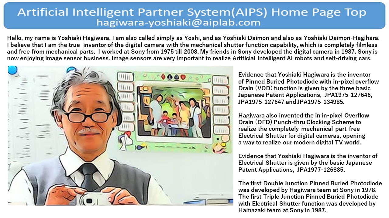
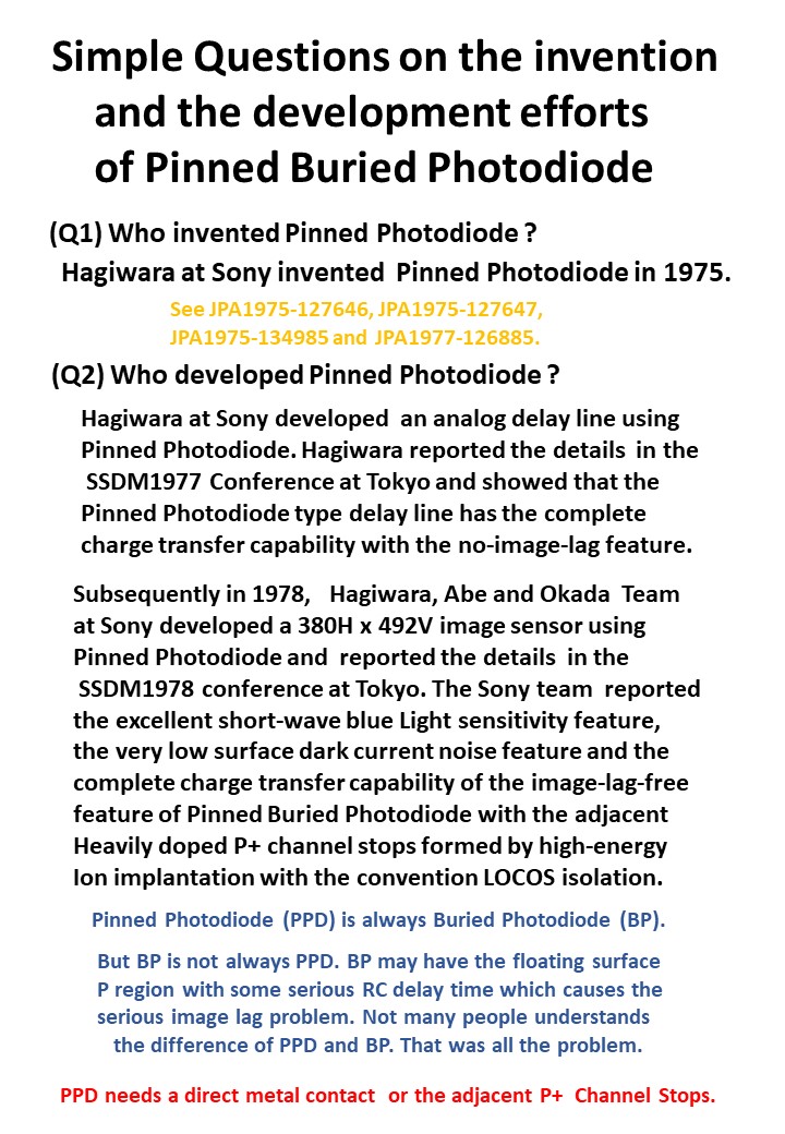
Who invented Pinned Photodiode ?
Hagwiara at Sony invented Pinned Buried Photodiode in 1975.
Who invented Electrical Shutter for the film-less digital imaging modern world ?
Hagwiara at Sony invented Electrical Shutter in 1975.
Who invented Global Shutter which is needed to surpress the Rotary Shutter Effect of the CMOS image sensors ?
Hagwiara at Sony invented Global Shutter in 1975.
+++++++++++++++++++++++++++++++++++++++++++++++++++++++++
index_introduction_to_Activities_of_Yoshiaki_Daimon_Hagiwara.html (in Japanese)
+++++++++++++++++++++++++++++++++++++++++++++++++++++++++
The_truth_about_the_Invention_of_Pinned_Photodiode.pdf
The_truth_about_the_Invention_of_Pinned_Photodiode_32min_52sec.mp4
The_truth_about_the_Invention_of_Pinned_Photodiode_Japanese_51min_13sec.mp4
+++++++++++++++++++++++++++++++++++++++++++++++++++++++++
The_truth_about_the_Invention_of_Pinned_Photodiode_1.pdf
The_truth_about_the_Invention_of_Pinned_Photodiode_2.pdf
The_truth_about_the_Invention_of_Pinned_Photodiode_3.pdf
The_truth_about_the_Invention_of_Pinned_Photodiode_4.pdf
++++++++++++++++++++++++++++++++++++++++++++++
+++++++++++++++++++++++++++++++++++++++++++++++++++++++++
Sony_1987_Image_Sensor_with_Electrical_Shutter_Function_invented_in_1975_by_Hagiwara.pdf
+++++++++++++++++++++++++++++++++++++++++++++++++++++++++
+++++++++++++++++++++++++++++++++++++++++++++++++++++++++
https://en.wikipedia.org/wiki/Yoshiaki_Hagiwara
https://en.wikipedia.org/wiki/Photodiode#Pinned_photodiode
https://www.sony.com/en/SonyInfo/News/notice/20200626/
https://www.shmj.or.jp/english/pdf/dis/exhibi1005E.pdf
https://electronics.stackexchange.com/questions/83018/difference-between-buried-photodiode-and-pinned-photodiode
https://openjurist.org/181/f3d/1313/loral-fairchild-corporation-v-sony-corporation-and-sony-electronics-incs
++++++++++++++++++++++++++++++++++++++++++++++
IEDM2005 Paper on Hole Role by Albert Thuewissen
https://harvestimaging.com/pubdocs/089_2005_dec_IEDM_hole_role.pdf
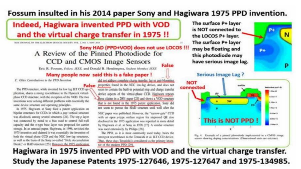
A Review of the Pinned Photodiode for CCD and CMOS Image Sensors by Erric Fossum
https://ieeexplore.ieee.org/stamp/stamp.jsp?tp=&arnumber=6742594
++++++++++++++++++++++++++++++++++++++++++++++
++++++++++++++++++++++++++++++++++++++++++++++++++++++++
Evidence_explaining_that_Hagiwara_at_Sony_is_the_inventor_of_Pinned_Photodiode.html
++++++++++++++++++++++++++++++++++++++++++++++++++++++++
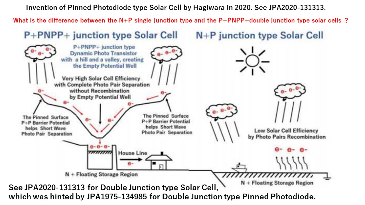
Pinned_Photodiode_type_Sola_Cell.pdf
Hagiwara_at_Sony_invented_in_1975_PNP_type_Pinned_Photodiode.pdf
++++++++++++++++++++++++++++++++++++++++++++++++++++++++
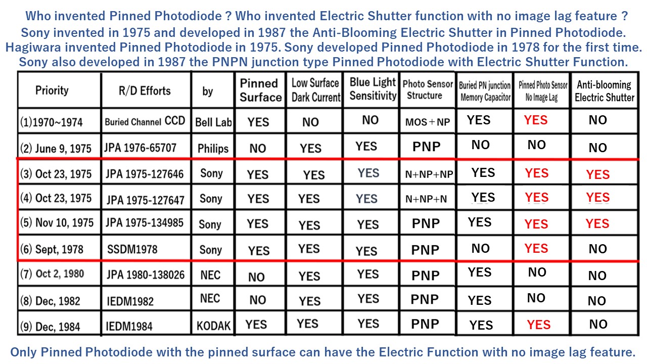
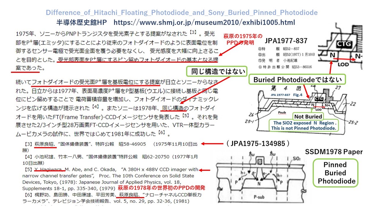
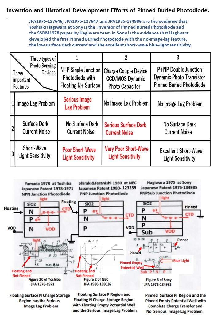
Papers related to the invention and the development efforts of Pinned Buried Photodiode.
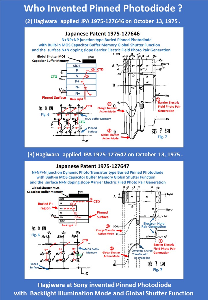
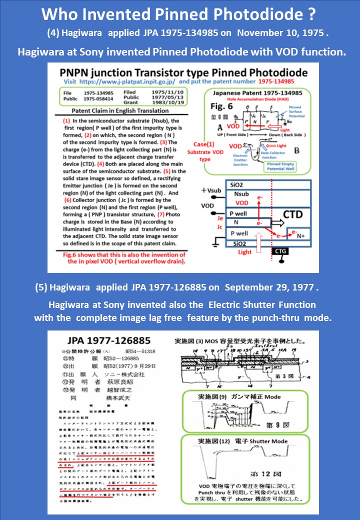
(A) The evidence that Hagiwara at Sony invented the NPN variant of Pinned Photodiode (PPD)
with the global shutter function is given by the Japanese patent applications,
JPA1975-127646[A1] and JPA1975-127647[A2]
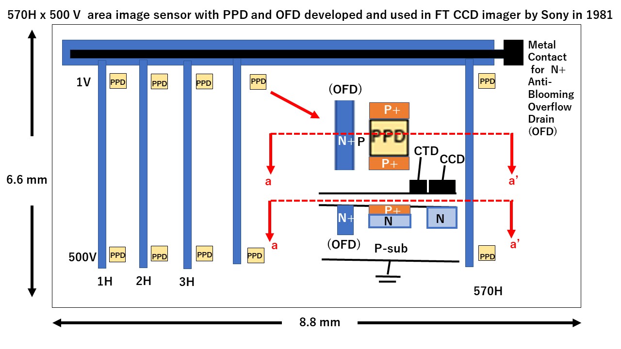
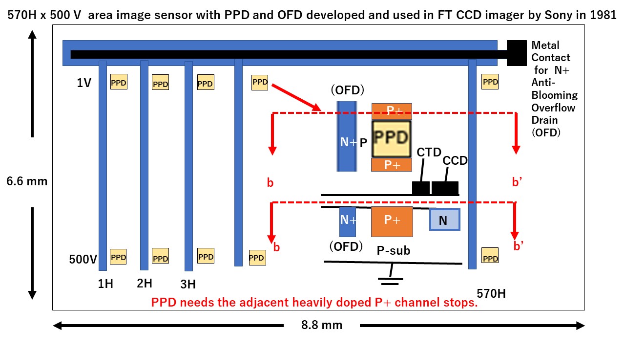
The evidence that Hagiwara at Sony invented the PNP type Pinned Photodiode (PPD)
with the in-pixel vertical overflow drain (VOD) anti-blooming structure is given by
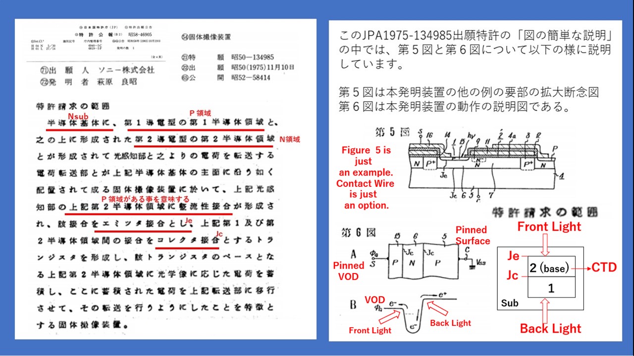
the Japanese patent applications, JPA1975-134985[A3]
(B) The evidence that Hagiwara at Sony developed the first PNP type PPD used in a delay line
is given by the SSDM1977 paper [B1] and used in the FT CCD area sensor given by the SSDM1978 paper [B2]
++++++++++++++++++++++++++++++++++++++++++++++++++++++++++++++++
Just for your information and for your further understandings
++++++++++++++++++++++++++++++++++++++++++++++++++++++++++++++++
(C) Hagiwara was invited at many international technical conference for his works.
And presented eight invited conference papers, [C1] thru [C8].
(D) Recently Hagiwara presented five papers, [D1] thru[D5] to explain the details of
the 1975 invention and the 1978 development effort of Pinned Photodiode for
the English speaking IEEE community for the first time.
+++++++++++++++++++++++++++++++++++++++++++++++++++
The information below is a list of publications with the link to the PDF files.
+++++++++++++++++++++++++++++++++++++++++++++++++++
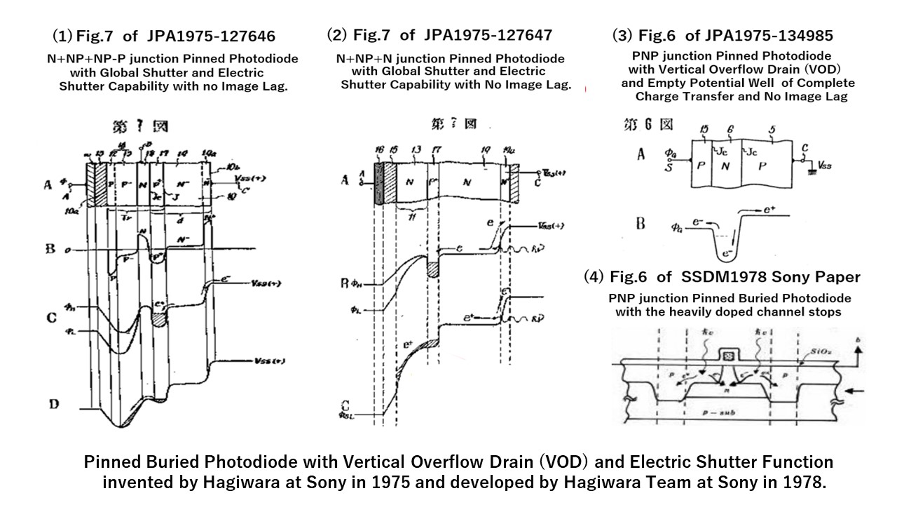
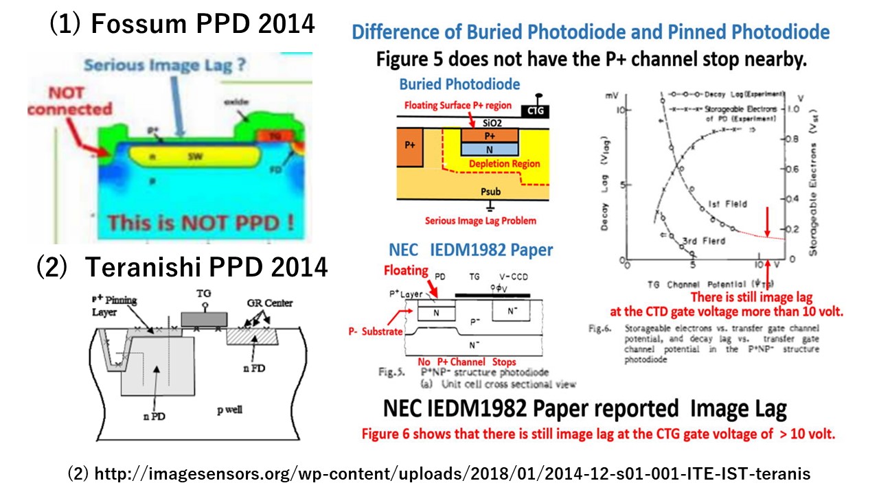
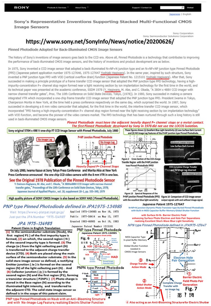
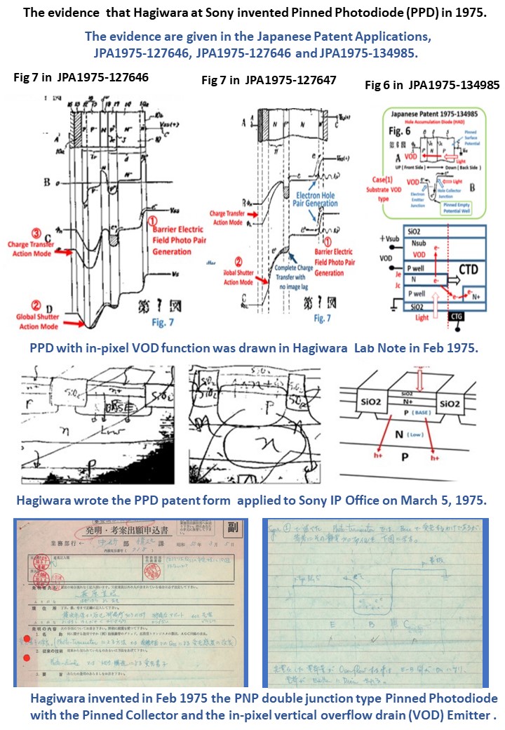
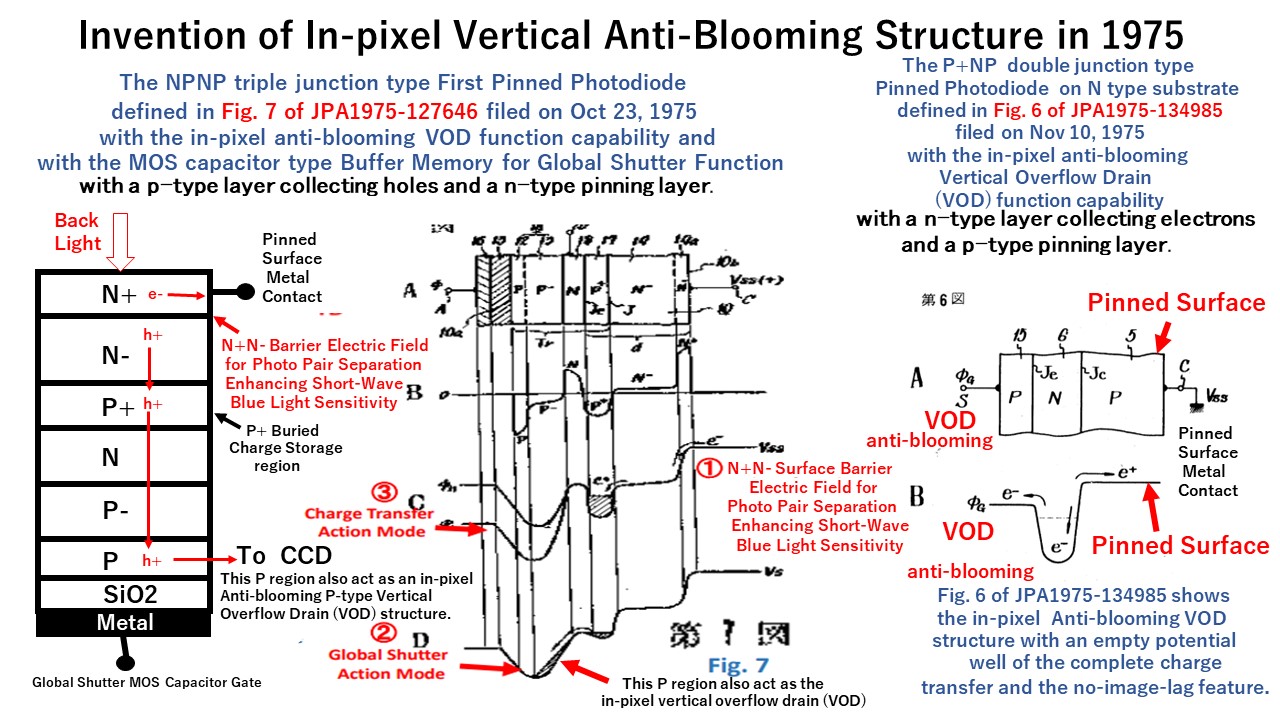
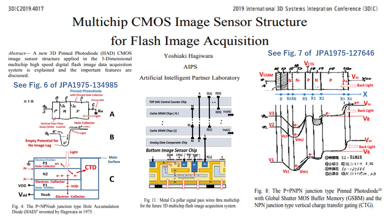
[A1] See Fig. 6 of JPA197-127646 on the triple junction N+NPNP variant of PPD with no image lag problem by the PNP junction type punch-thru action also with Global Shutter Structure with the pinned N+N surface with the surface N+N induced barrier electric field, enhancing the surface photo electron and hole separations for the short-wave blue light sensitivity to realize the super light sensitive video cameras.
3_JP1975-127646_NPNP_triple_junction_Pinned_Photodiode_Patent_32_pages.pdf
[A2] See Fig. 6 of JPA197-127647 on the triple junction N+NPN variant of PPD with no image lag problem by the PN junction type punch-thru action also with Global Shutter Structure with the pinned N+N surface with the surface N+N induced barrier electric field, enhancing the surface photo electron and hole separations for the short-wave blue light sensitivity to realize the super light sensitive video cameras.
4_JP1975-127647_NPN_double_junction_Pinned_Photodiode_Patent_22_pages.pdf
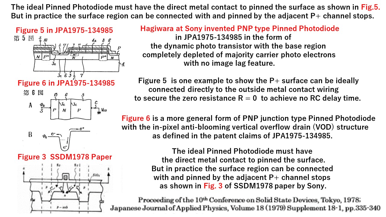
[A3] See fig. 6 of JPA1975-134985 which defined the PNP junction type pinned photodiode with the PN collector junction used for the photo electron and hole pair separation at the pinned p surface and with the NP emitter junction used the anti-blooming diode structure.
5_JP1975-134985_PNP_double_junction_Pinned_Photodiode_on_Nsub_Patent_7_pages.pdf
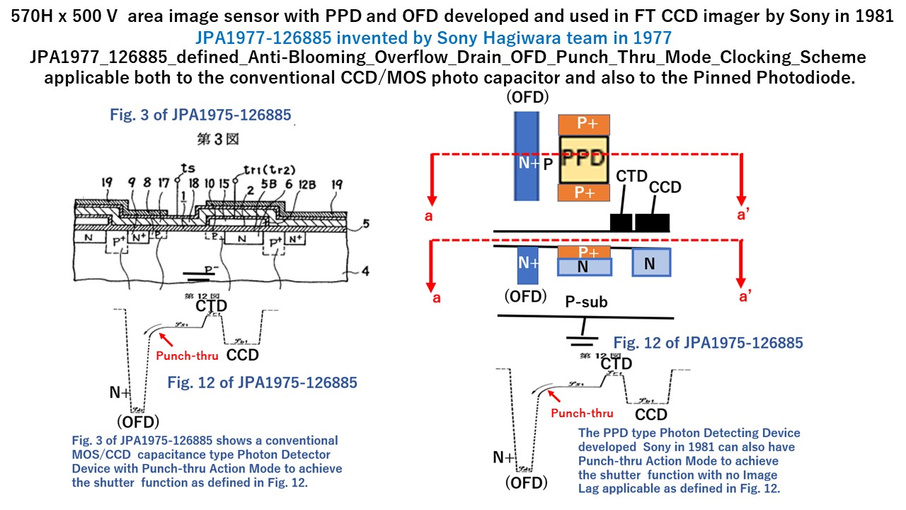
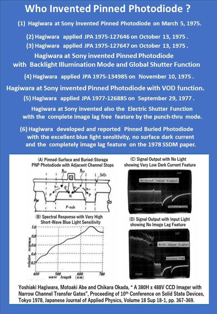
[B1] The evidence that Hagiwara developed the first PNP type Pinned Photodiode as a delay line with complete charge transfer is given by Sony in SSDM1977 paper for the first time in the world.
Y. Daimon-Hagiwara Proc. 9 th Conf. on Solid-State Devices, Tokyo, 1977, pp.335-340,
P1977_SSDM1977_Paper_on_Narrow_Channel_CCD_with_P+NP_Junction_Photodiode.pdf
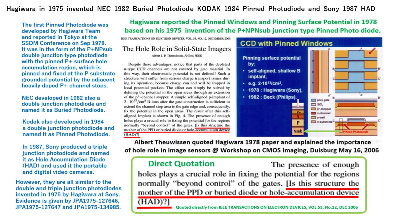
[B2] The evidence that Hagiwara developed the first PNP type Pinned Photodiode is given by Sony in SSDM1978 paper with no image lag problem reported PPD used in FT CCD for the first time in the world.
Y. Daimon-Hagiwara et.al., Proc. 10th Conf. on Solid-State Devices, Tokyo, 1978, pp.335-340,
P1978_Pinned_Photodiode_1978_Paper_by_Hagiwara.pdf
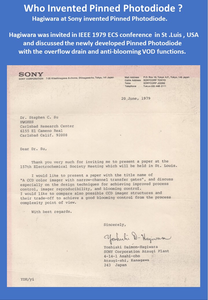
[C1] Invited Paper at the CCD79 conference in Edinburgh, Scotland UK
1979%20CCD79/03-1%20Hagiwara.pdf
[C2] Invited Paper at the ECS1980 conference at St. Luis USA
ECS1980_a_letter_of_reply_to_the_invitation_to_ECS1980_conference.pdf
[C3] Invited Paper at the ESSCIRC2001 Conference at Vilach, Autria
P2001_ESSCIRC2001.pdf
[C4] Invited Tutorial Talk at the IEDM2004 Conference at San Francisco, USA
P2004_IEDM2004_1212_Short_Cource_on_Image_Sesnors_by_Yoshiaki_Hagiwara.pdf
[C5] Invited Paper at the ESSCIRC2008 Conference at Edinburgh, Scotland, UK
P2008_ESSCIRC2008Hagiwara.pdf
[C6] Invited Paper at the ICD2008 Conference in Tokyo, Japan on Dec 12, 2008
ICD2008_Conference_Invited_Paper_on_Dec_12_2008_on_Prospect_of_Developing_AIP_Robot_for_Home_Total_Supporting_Systems.pdf
[C7] Invited Paper at the Cool Chips Conference at Yokohama, Japan
CoolChipsPanelTalk20170420.pdf
[C8] Invited Plenary Panel Talk in ISSCC2013 conference, San Francisco, USA
13_P2013_ISSCC2013_Panel_Talk_25_pages.pdf
[D1] P2019_3DIC2019 Conference Paper on "Multichip CMOS Image Sensor Structure for Flash Image Acquisition"
P2019_3DIC2019Paper_on_3D_Pinned_Photodiode.pdf
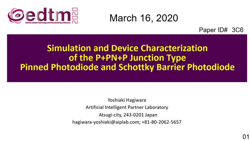
[D2] P2020_EDTM2020 Conference Paper on "Simulation and Device Characterization of the P+PN+P Junction Type Pinned Photodiode and Schottky Barrier Photodiode "
P2020_EDTM2020_PaperID_3C4_by_Hagiwara.pdf
[D3] P2021_IJSSA2021_e-Journal Paper on "Electrostatic and Dynamic Analysis of P+PNP Double Junction Type and P+PNPN Triple Junction Type Pinned Photodiodes"
P2021_IJSSA2021_Paper_20210616_on_Electrostatic_and_Dynamic_Analysis_of_Pinned_Photodiodes.pdf
[D4] ICECET2021_Conference_Paper061 on "Pinned Buried PIN Photodiode Type Solar Cell"
001A_ICECET2021_Paper061_Pinned_Buried_PIN_Photodiode_type_Solar_Cell.pdf
[D5] ICECET2021_Conference_Paper075 on "Invention and Historical Development Efforts of Pinned Buried Photodiode "
002A_ICECET2021_Paper075_Invention_and_Historical_Development_Efforts_of_Pinned_Buried_Photodiode.pdf
+++++++++++++++++++++++++++++++++++++++++++++++++++++
With these published papers, I really wish to help editors understand my invention
and my development efforts so that I would have their kind supports.
+++++++++++++++++++++++++++++++++++++++++++++++++++++
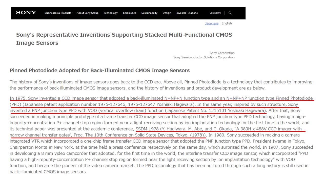
Sony publically annouced that Hagiwara at Sony invented Pinned Photodiode in 1975 (pdf)
++++++++++++++++++++++++++++++++++++++++++++++
Evidence_that_Hagiwara_at_Sony_is_the_inventor_of_Pinned_Photodiode.html
Evidence_that_Hagiwara_at_Sony_invented_Pinned_Buroed_Photodiode_with_in_Pixel_VOD_in_1975.pdf
++++++++++++++++++++++++++++++++++++++++++++++
Image_Sensor_Story_07.pdf
++++++++++++++++++++++++++++++++++++++++++++++
Pinned_Photodiode_with_anti_blooming_OFDstrucuture_invente_by_hagiwara_and_use_by_Sony_in_1981.pdf
++++++++++++++++++++++++++++++++++++++++++++++
Pinned_Photodiode_with_anti_blooming_OFD_strucuture_invente_by_hagiwara_and_use_by_Sony_in_1981_Slide01.pdf
++++++++++++++++++++++++++++++++++++++++++++++
Pinned_Photodiode_with_anti_blooming_OFD_strucuture_invente_by_hagiwara_and_use_by_Sony_in_1981_Slide02.pdf
++++++++++++++++++++++++++++++++++++++++++++++
Pinned_Photodiode_with_anti_blooming_OFD_strucuture_invente_by_hagiwara_and_use_by_Sony_in_1981_Slide03.pdf
++++++++++++++++++++++++++++++++++++++++++++++
Pinned_Photodiode_with_anti_blooming_OFD_strucuture_invente_by_hagiwara_and_use_by_Sony_in_1981_Slide04.pdf
++++++++++++++++++++++++++++++++++++++++++++++
index_Japanes.html
index_Japanese_001.html
index_Japanese_002.html
index_Japanese_003.html
index_Japanese_004.html
index_Japanese_005.html
index_Japanese_006.html
index_Japanese_007.html
index_Japanese_008.html
Back_up_List of aiplab.com Past Home Pages
++++++++++++++++++++++++++++++++++++++++++++++
2006_dec_TED_hole_role.pdf_by_Albert_Thewissen.pdf
SSDM1978_Paper_(pdf)_on_the_first_Pinned_Photodiode_developed_by_Hagiwara_at_Sony
https://www.sony.com/en/SonyInfo/News/notice/20200626/
++++++++++++++++++++++++++++++++++++++++++++++
How_to_find_JPA1975_127646_Patent_from_Official_Japan_Patent_Office_WEB_site_2022_02_10.pdf
JPA1975-127646_on_NPNP_triple_junction_Pinned_Photodiode_with_the_MOS_Buffer_Memory_for_Global_Shutter_Function.pdf
JPA1975-127647_on_NPN_double_junction_Pinned_Photodiode_with_the_MOS_Buffer_Memory_for_Global_Shutter_Function.pdf
JPA1975-134985_on_PNP_double_junction_Pinned_Photodiode_with_Vertical_OFD_(VOD)_function
++++++++++++++++++++++++++++++++++++++++++++++
List of Content
++++++++++++++ New High Light ++++++++++++++++
Evidence_that_Hagiwara_at_Sony_is_the_inventor_of_Pinned_Photodiode.html
Who_invented_Pinned_Photodiode_by_Hagiwara.pdf
++++++++++++++++++++++++++++++++++++++++++++++
Japanese Diary Essay by Yoshiaki Hagiwara in 1964 at age 15
Candy_in_the_Heart.html
Hagiwara Yoshiaki Daily Mumbling ( Voice Diary in Japanese )
Oh_Sony_My_Life_by_Yoshiaki_Daimon_Hagiwara.html
++++++++++++++++++++++++++++++++++++++++++++++
About the First Pnysics Book Hagiwara studied at Caltech in 1967 at age 18
Review_on_the_Feynman_Lectures_of_Physics.html
About the major contribution of Yoshiaki Hagiwara on Japan Semiconductor Industry at age 26
Review_on_Invention_of_Pinned_Photodiode.html
About the life work of Yoshiaki Hagiwara on AIPS and AI Robotics
World_of_Digital_Circuits_for_AIPS.html
++++++++++++++++++++++++++++++++++++++++++++++
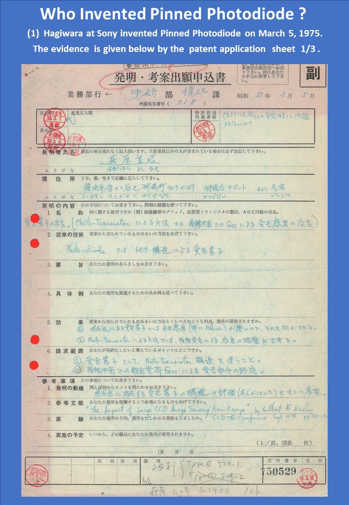
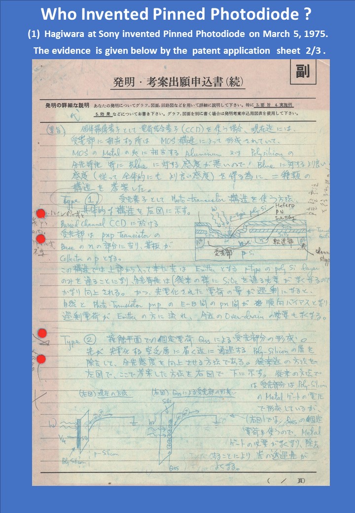
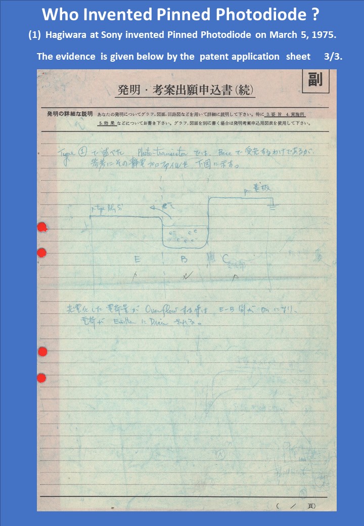
Yoshiaki Hagiwara at Sony invented Pinned_Photodiode on March 5, 1975
Who_Invented_Pinned_Photodiode_in_Japanese.pdf
++++++++++++++++++++++++++++++++++++++++++++++
Publication_List_by_Yoshiaki_Hagiwara.html
++++++++++++++++++++++++++++++++++++++++++++++
Who_Invented_Pinned_Photodiode.pdf
+++++++++++++++++++++++++++++++++++++++++++
++++++++++++++++++++++++++++++++++++++++++++++
ICECET2021_Paper061_and_Paper075.html
++++++++++++++++++++++++++++++++++++++++++++++
Please write me freely at hagwiara-yoshiaki@aiplab.com
++++++++++++++++++++++++++++++++++++
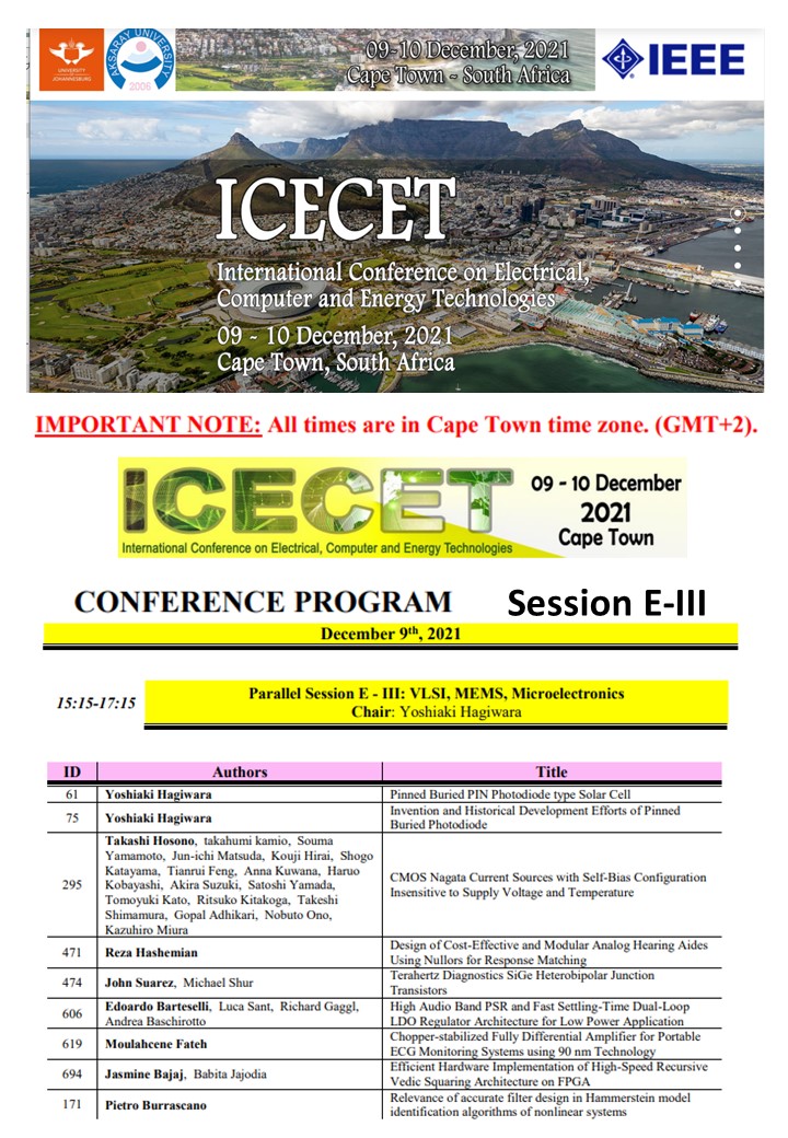
http://www.icecet.com/home
http://www.icecet.com/ICECET_Program.pdf
ICECET2021_Session_E-III_chaired_by_Yoshiaki_Hagiwara.pdf
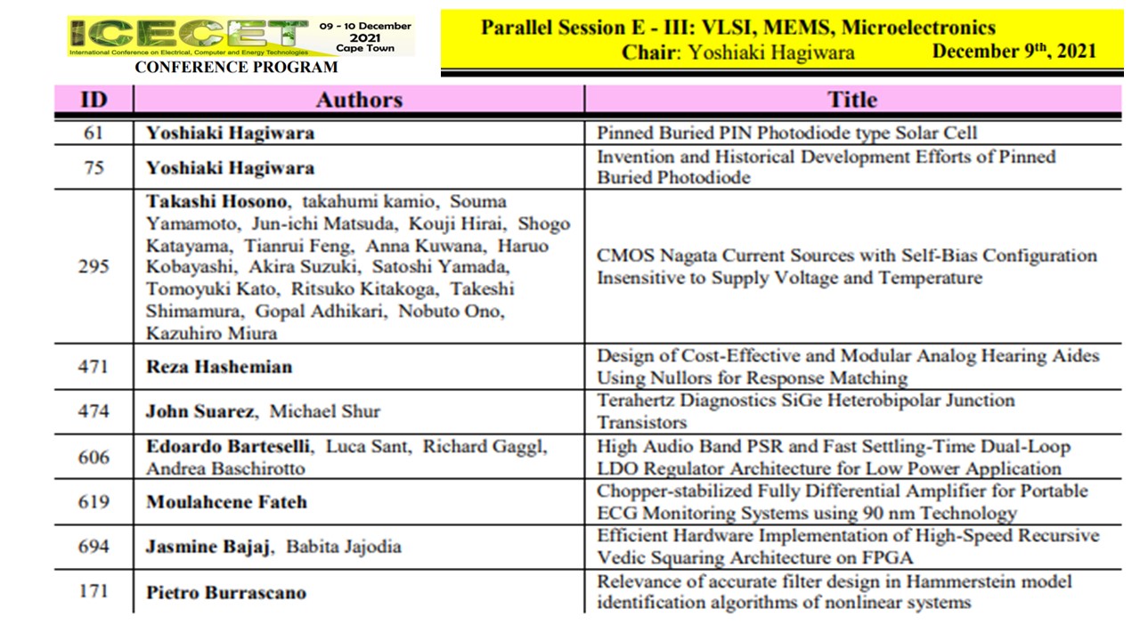
ICECET2021_Program_Session_E-III.pdf
++++++++++++++++++++++++++++++++++++
The presentation slides, pdf, mp3 audio and mp4 video files
of my papers 061 and 075 are now all uploaded into:
ICECET2021_Paper61_html
ICECET2021_Paper75_html
held at the IEEE ICECET2021 conference
in Cape Town, South Afrrica on Dec 9 and 10, 2021.
http://www.icecet.com/home
http://www.icecet.com/ICECET_Program.pdf
ICECET2021_Session_E-III_chaired_by_Yoshiaki_Hagiwara.pdf
*************************************************************
001A_ICECET2021_Paper061_Pinned Buried PIN Photodiode type Solar Cell.pdf
001B_ICECET2021_acceptance_letter_ID_061.pdf
001C_ICECET 2021_PARTICIPATION_CERTIFICATE_061.pdf
001D_ICECET2021_Paper061_supplement_Process_Flow_of_Pinned_Buried_PIN_Photodiode_type_Solar_Cell_2021_08_14.pdf
002A_ICECET2021_Paper075_Invention and Historical Development Efforts of Pinned Buried Photodiode.pdf
002B_ICECET2021_acceptance_letter_ID_075.pdf
002C_ICECET 2021 PARTICIPATION CERTIFICATE_075.pdf
002D_ICECET2021_Paper075_supplement_The_Evidence_that_Hagiwar_at_Sony_invente_Pinne_Burie_Photodiode_in_1975.pdf
003_ICECET2021_CHAIR_CERTIFICATE_Session_E3.pdf
004_ICECET2001_Session_E-III_Chaired_by_Yoshiaki_Hagiwara.pdf
*************************************************************
IEEE_P2019_3DIC2019_Paper_on_3D_Pinned_Photodiode_6_pages.pdf
IEEE_2019_International_3D_Systems_Integration_Conference_Paper_by_Hagiwara_AIPS.pdf
+++++++++++++++++++++++++++++++++++++++++++
*************************************************************
P2021_IJSSA2021_Paper_June_16_2021_on_Electrostatic_and_Dynamic_Analysis_of_Pinned_Photodiodes_22_Pages.pdf
P2021_IJSSA2021_Paper_June_16_2021_on_Electrostatic_and_Dynamic_Analysis_of_Pinned_Photodiodes.pdf
https://www.sciencepublishinggroup.com/journal/paperinfo?journalid=245&doi=10.11648/j.ijssam.20210602.13
+++++++++++++++++++++++++++++++++++++++++++
*************************************************************
EDTM2020_Conference_Paper_on_Slide001.html
*************************************************************
Invention_an_Historical_Developmen_Efforts_of_Pinne_Burie_Photodiode.pdf
+++++++++++++++++++++++++++++++++++++++++++
*************************************************************
+++++++++++++++++++++++++++++++++++++++++++++++++++++++++
index_introduction_to_Activities_of_Yoshiaki_Daimon_Hagiwara.html (in Japanese)
+++++++++++++++++++++++++++++++++++++++++++++++++++++++++